- 您现在的位置:买卖IC网 > Sheet目录2011 > MAX5893EGK+D (Maxim Integrated Products)IC DAC 12BIT DUAL 500MSPS 68-QFN
MAX5893
For stable operation with the internal reference, REFIO
should be decoupled to GND with a 1F capacitor.
REFIO must be buffered with an external amplifier, if
heavy loading is required, due to its 10k
output resis-
tance.
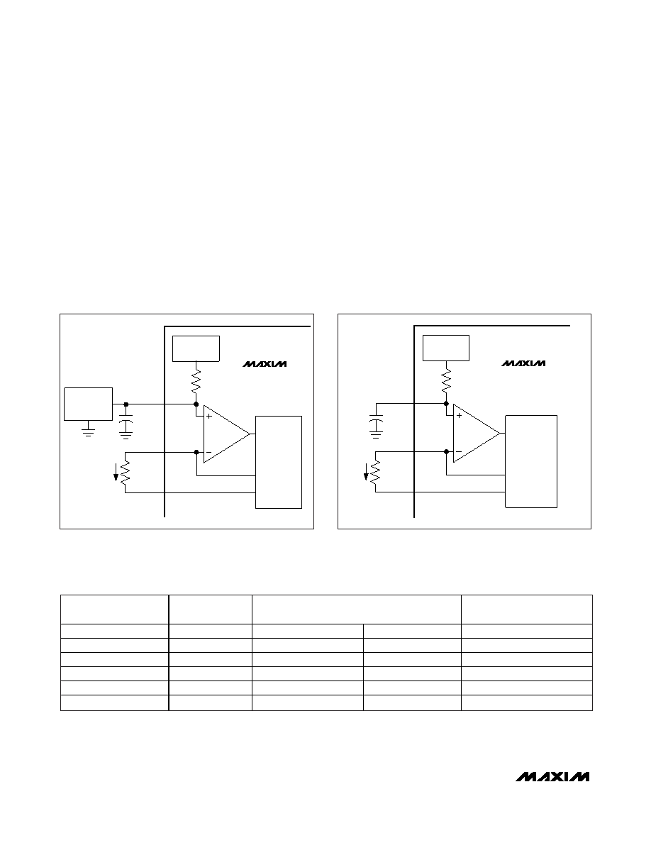
Alternatively, apply a temperature-stable external refer-
ence to REFIO (Figure 18). The internal reference is over-
driven by the external reference. For improved accuracy
and drift performance, choose a fixed output voltage ref-
erence such as the MAX6520 bandgap reference.
The MAX5893’s reference circuit (Figure 19) employs a
control amplifier, designed to regulate the full-scale
current IOUT for the differential current outputs of the
DAC. The output current can be calculated as:
IOUTFS = 32 x IREFIO - 1LSB
IOUTFS = 32 x IREFIO - (IOUT/212)
where IREFIO is the reference output current (IREFIO =
VREFIO/RSET) and IOUT is the full-scale output current
of the DAC. Located between FSADJ and DACREF,
RSET is the reference resistor, which determines the
amplifier’s output current for the DAC. Use Table 5 for a
matrix of different IOUTFS and RSET selections.
12-Bit, 500Msps Interpolating and Modulating
Dual DAC with CMOS Inputs
28
______________________________________________________________________________________
Figure 18. Typical External Reference Circuit
1.2V
REFERENCE
CURRENT-
SOURCE
ARRAY DAC
REFIO
EXTERNAL
1.25V
REFERENCE
RSET
FSADJ
IREF
10k
DACREF
1
F
MAX5893
1.2V
REFERENCE
CURRENT-
SOURCE
ARRAY DAC
REFIO
FSADJ
IREF
10k
DACREF
1
F
MAX5893
RSET
FULL-SCALE
CURRENT
REFERENCE
CURRENT
RSET (
)
OUTPUT VOLTAGE
IOUTFS (mA)
IREF (A)
CALCULATED
1% EIA STD
VIOUTP/N* (mVP-P)
2
62.50
19.2k
19.1k
100
5
156.26
7.68k
7.5k
250
10
312.50
3.84k
3.83k
500
15
468.75
2.56k
2.55k
750
20
625.00
1.92k
1.91k
1000
Figure 19. MAX5893 Internal Reference Architecture
Table 5. IOUTFS and RSET Selection Matrix Based on a Typical 1.20V Reference Voltage
*
Terminated into a 50
load.
发布紧急采购,3分钟左右您将得到回复。
相关PDF资料
MAX5894EGK+D
IC DAC 14BIT DUAL 500MSPS 68-QFN
MAX5895EGK+D
IC DAC 16BIT 500MSPS DUAL 68-QFN
MAX5898EGK+D
IC DAC 16BIT DUAL 500MSPS 68-QFN
MAX6900ETT+T
IC RTC I2C COMPAT 6-TDFN
MAX6902ETA+T
IC RTC SPI COMPAT 8-TDFN
MAX7375AXR604+T
IC OSC SILICON SC70-3
MAX7394ATTLY+T
IC OSC SILICON 922KHZ 6-TDFN
MAX7403CSA+
IC FILTER LOWPASS 8-SOIC
相关代理商/技术参数
MAX5893EGK+TD
功能描述:数模转换器- DAC 12-Bit 2Ch 500Msps DAC RoHS:否 制造商:Texas Instruments 转换器数量:1 DAC 输出端数量:1 转换速率:2 MSPs 分辨率:16 bit 接口类型:QSPI, SPI, Serial (3-Wire, Microwire) 稳定时间:1 us 最大工作温度:+ 85 C 安装风格:SMD/SMT 封装 / 箱体:SOIC-14 封装:Tube
MAX5893EGK-D
功能描述:数模转换器- DAC RoHS:否 制造商:Texas Instruments 转换器数量:1 DAC 输出端数量:1 转换速率:2 MSPs 分辨率:16 bit 接口类型:QSPI, SPI, Serial (3-Wire, Microwire) 稳定时间:1 us 最大工作温度:+ 85 C 安装风格:SMD/SMT 封装 / 箱体:SOIC-14 封装:Tube
MAX5893EGK-TD
功能描述:数模转换器- DAC RoHS:否 制造商:Texas Instruments 转换器数量:1 DAC 输出端数量:1 转换速率:2 MSPs 分辨率:16 bit 接口类型:QSPI, SPI, Serial (3-Wire, Microwire) 稳定时间:1 us 最大工作温度:+ 85 C 安装风格:SMD/SMT 封装 / 箱体:SOIC-14 封装:Tube
MAX5893EVCMOD2
功能描述:数模转换器- DAC Evaluation Kit for the MAX5893/MAX5894/MAX5895 RoHS:否 制造商:Texas Instruments 转换器数量:1 DAC 输出端数量:1 转换速率:2 MSPs 分辨率:16 bit 接口类型:QSPI, SPI, Serial (3-Wire, Microwire) 稳定时间:1 us 最大工作温度:+ 85 C 安装风格:SMD/SMT 封装 / 箱体:SOIC-14 封装:Tube
MAX5893EVKIT
功能描述:数模转换器- DAC Evaluation Kit for the MAX5893/MAX5894/MAX5895 RoHS:否 制造商:Texas Instruments 转换器数量:1 DAC 输出端数量:1 转换速率:2 MSPs 分辨率:16 bit 接口类型:QSPI, SPI, Serial (3-Wire, Microwire) 稳定时间:1 us 最大工作温度:+ 85 C 安装风格:SMD/SMT 封装 / 箱体:SOIC-14 封装:Tube
MAX5894EGK+D
功能描述:数模转换器- DAC 14-Bit 2Ch 500Msps DAC RoHS:否 制造商:Texas Instruments 转换器数量:1 DAC 输出端数量:1 转换速率:2 MSPs 分辨率:16 bit 接口类型:QSPI, SPI, Serial (3-Wire, Microwire) 稳定时间:1 us 最大工作温度:+ 85 C 安装风格:SMD/SMT 封装 / 箱体:SOIC-14 封装:Tube
MAX5894EGK+TD
功能描述:数模转换器- DAC 14-Bit 2Ch 500Msps DAC RoHS:否 制造商:Texas Instruments 转换器数量:1 DAC 输出端数量:1 转换速率:2 MSPs 分辨率:16 bit 接口类型:QSPI, SPI, Serial (3-Wire, Microwire) 稳定时间:1 us 最大工作温度:+ 85 C 安装风格:SMD/SMT 封装 / 箱体:SOIC-14 封装:Tube
MAX5894EGK-D
功能描述:数模转换器- DAC RoHS:否 制造商:Texas Instruments 转换器数量:1 DAC 输出端数量:1 转换速率:2 MSPs 分辨率:16 bit 接口类型:QSPI, SPI, Serial (3-Wire, Microwire) 稳定时间:1 us 最大工作温度:+ 85 C 安装风格:SMD/SMT 封装 / 箱体:SOIC-14 封装:Tube